BIGNANOTECH is Transforming Environmental Remediation in Vietnam
BIGNANOTECH is revolutionizing environmental remediation in Vietnam with advanced nanotechnology, delivering sustainable solutions to purify soil, water, and air. Products like N-Biopowder, oil-absorbent pads, oil-absorbent booms, and meltblown antibacterial fabric harness nano-particles and native microorganisms to combat pollution effectively, paving the way for a greener Vietnam. This innovative approach addresses the country’s unique environmental challenges, from industrial waste to coastal oil spills. Learn more about nano-based technology fundamentals at Nano.gov.
Discover BIGNANOTECH’s nano solutions

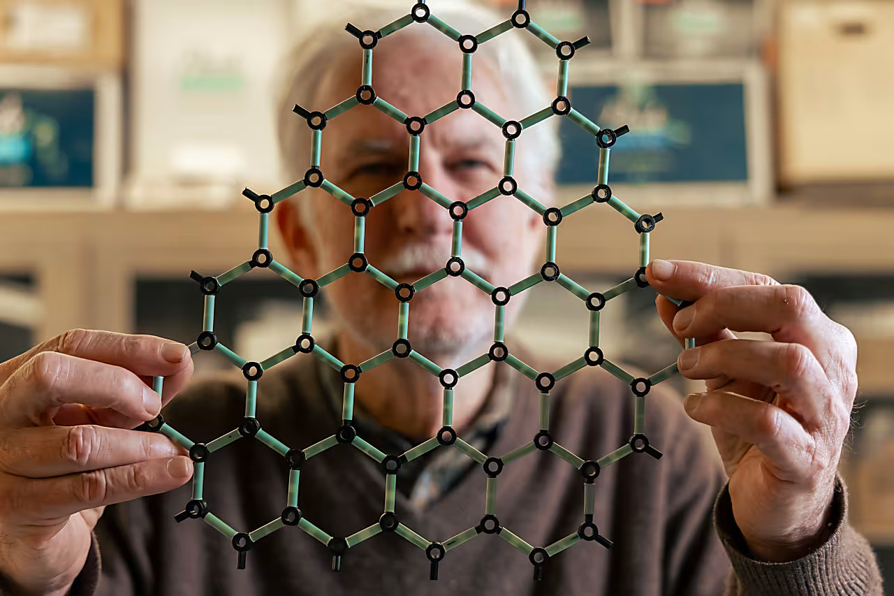
BIGNANOTECH nanotechnology lab developing environmental solutions in Vietnam
What is Nanotechnology?
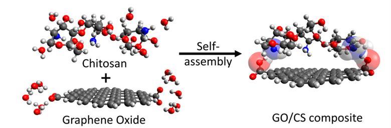
Nanotechnology utilizes particles smaller than 100nm to tackle environmental challenges at the molecular level. At BIGNANOTECH, nano-solutions is engineered to provide:
- Deep Penetration: Nano-particles access hard-to-reach contaminated zones.
- Rapid Degradation: Eliminates pollutants like oil, heavy metals, and chemicals.
- Eco-Friendly: Generates no harmful byproducts, protecting ecosystems.
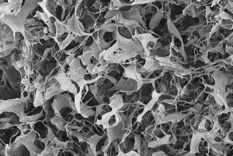
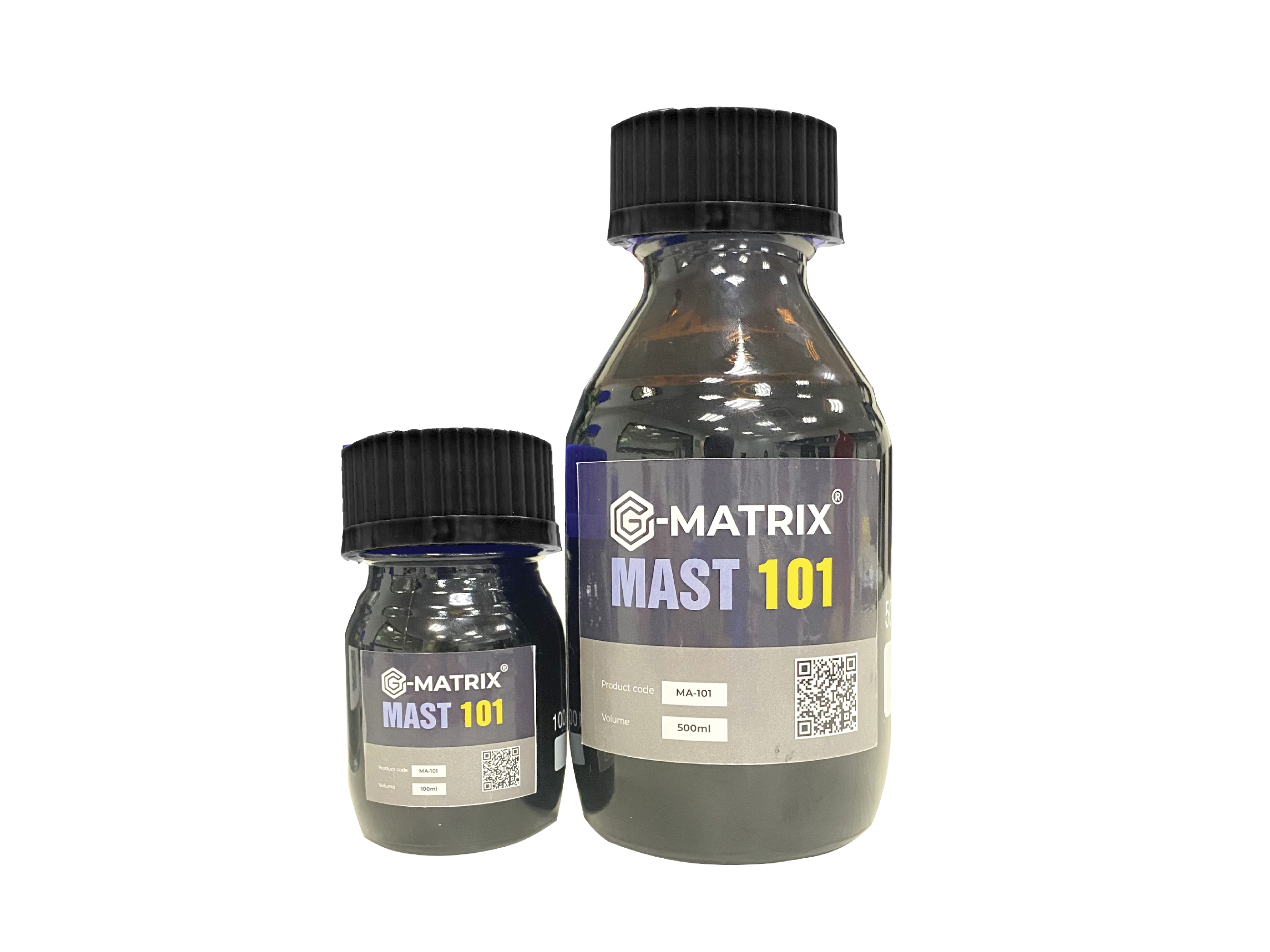
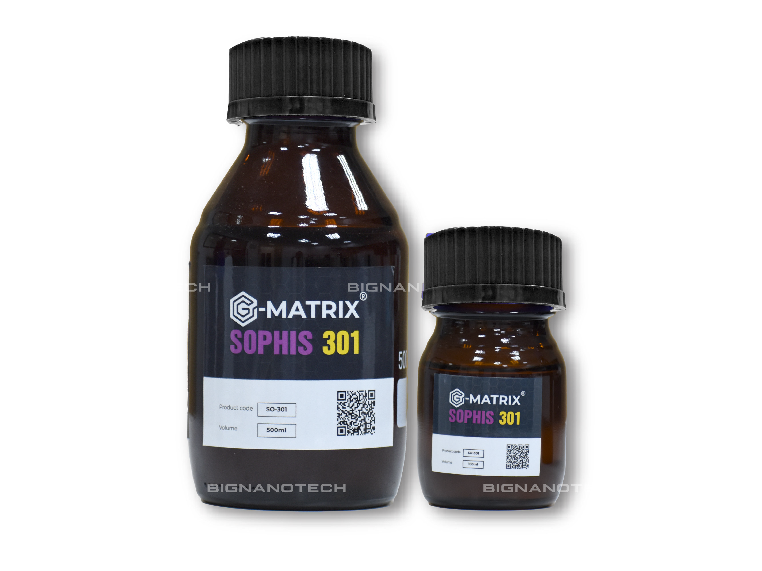
For example, N-Biopowder integrates nano-particles with microorganisms (Pseudomonas, Rhodococcus) to degrade 68% of petroleum hydrocarbons, restoring fertile soil in affected areas.
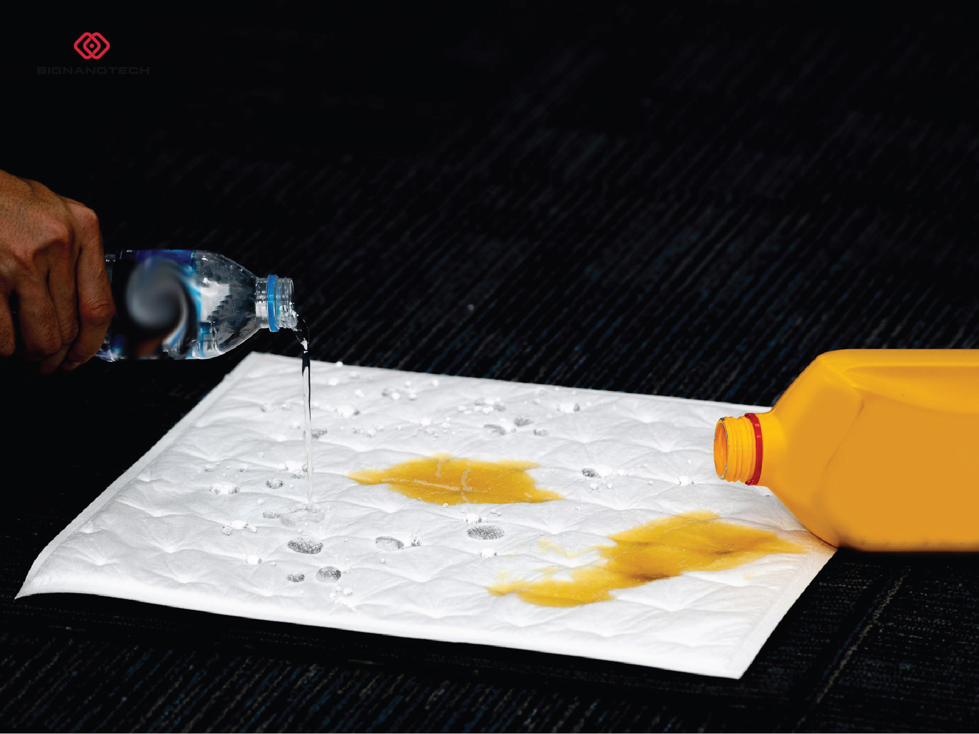
Similarly, oil-absorbent pads and booms leverage nanotechnology to enhance absorption, efficiently managing oil spills along Vietnam’s coastal regions. This demonstrates how nanotechnology’s core principles are applied in real-world scenarios.
Learn more about BIGNANOTECH’s nanotechnology
Applications of Nanotechnology in Vietnam
BIGNANOTECH applies nano-tech to address Vietnam’s critical environmental issues:
- Oil-Contaminated Soil Remediation: Products like N-Biopowder restore agricultural land impacted by oil spills in regions like Vung Tau and Quang Ngai, revitalizing farming communities.
- Water Purification: Nano-particles remove heavy metals and chemicals from industrial wastewater, ensuring safe water sources for local populations.
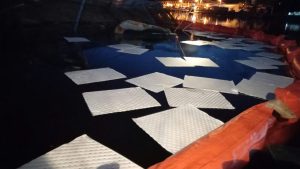
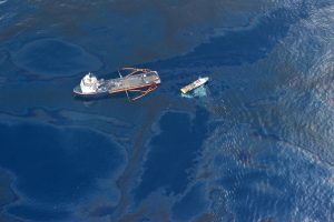
- Oil Spill Response: Oil-absorbent pads, booms, and oil absorbent cotton swiftly contain and clean oil spills at ports and industrial zones, minimizing ecological damage.
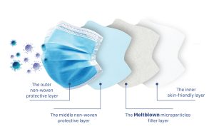
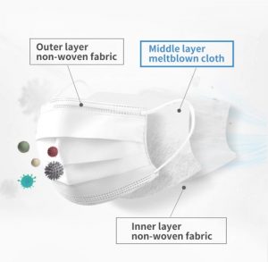
- Air Quality Improvement: Meltblown Antibacterial Fabric (BFE95, BFE99) is used in masks and filtration systems, enhancing public health in urban areas like Hanoi.
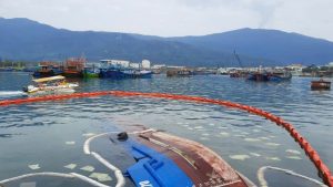
BIGNANOTECH oil-absorbent pads cleaning oil spill in Vung Tau, Vietnam
Manufactured at BIGNANOTECH’s cutting-edge facility in Thai Binh, these products are tailored to Vietnam’s unique environmental needs, reflecting local expertise and innovation.
Why BIGNANOTECH’s Nanotechnology Excels
Compared to traditional methods like chemical or thermal treatments, BIGNANOTECH’s nano-solutions offers superior benefits:
- High Efficiency: Degrades 68% of pollutants rapidly, meeting stringent environmental standards.
- Cost-Effective: Cuts cleanup costs by over 50% compared to conventional methods, benefiting industries and communities.
- Proudly Vietnamese: Developed by Vietnamese experts, optimized for local conditions and challenges.
- Sustainable: Safeguards soil, water, and air without secondary pollution, aligning with global green goals.
Products like N-Biopowder, oil-absorbent pads, and meltblown antibacterial fabric available on bignanotech.com showcase the power of nano-based technology in addressing Vietnam’s environmental challenges.
Nanotechnology for a Sustainable Vietnam
Vietnam faces significant pollution from industrial activities and oil spills, impacting agriculture, coastal ecosystems, and public health.
BIGNANOTECH’s nano-tech not only cleans contaminated environments but also supports sustainable agriculture and safe food production. For instance, in the South China Sea’s oil extraction zones, oil-absorbent booms and pads have restored coastal ecosystems, enabling farmers to resume cultivation with improved yields.
Meanwhile, meltblown antibacterial fabrics improve air quality in urban centers like Hanoi, enhancing community well-being by reducing respiratory issues. Explore global environmental efforts at UN Environment.
BIGNANOTECH’s innovative solutions are scalable, applicable from small farms to large industrial sites, making a tangible impact across Vietnam. Recent projects in Vung Tau have shown soil recovery rates 20% faster than traditional methods, while Hanoi’s air filtration pilots have lowered pollutant levels by 15%. By leveraging nano-tech, BIGNANOTECH is committed to building a cleaner, healthier future.
Act Now – Protect Vietnam’s Environment with BIGNANOTECH!
BIGNANOTECH’s nano-solutions are the key to tackling pollution and fostering a sustainable Vietnam. Explore products like N-Biopowder, oil-absorbent pads, and meltblown antibacterial fabric on bignanotech.com and contact us for a free consultation tailored to your environmental needs! Our team is ready to support your sustainability goals.
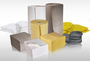
BIGNANOTECH environmental products like oil-absorbent pads, booms.
Contact Us
- Hotline: (+84) 879 808 080 | (+84) 868 939 595
- Website: bignanotech.com
- Email: sales@bignanotech.com
- Address: Tower A The Manor, Me Tri Street, My Dinh 1 Ward, Nam Tu Liem District, Hanoi, Vietnam
BIGNANOTECH – Pioneering nanotechnology for a sustainable Vietnam!