
In the evolution of electronic devices, silicon has always been dominant. However, with the continuous advancement of Moore’s Law, the physical limitations of silicon-based materials are becoming apparent. Today, we are on the brink of an industrial revolution, with various sectors exploring different materials, notably wide bandgap semiconductors like SiC and GaN. The latest buzz surrounds graphene.
Discovered in 2004 by two professors at the Chernogolovka Institute of Microelectronics at the University of Manchester, graphene has been hailed as a miracle material. Graphene, a two-dimensional material consisting of a single layer of carbon atoms, boasts three remarkable properties:
- It is extremely strong, being over 200 times stronger than steel.
- It has extremely high carrier mobility.
- It possesses very high thermal conductivity, allowing efficient heat dissipation and preventing electronic devices from overheating.
Graphene seems ideal for the electronics industry, but it lacks a bandgap, a crucial property for transistor switching. For the past 20 years, efforts have focused on “opening a gap” in graphene, the primary challenge for commercial applications.

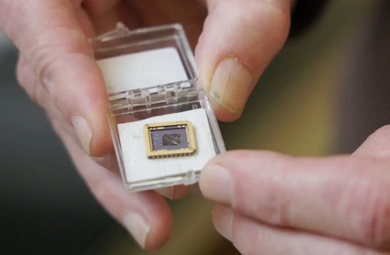
Recent research by Professor Walter de Heer’s group at the Georgia Institute of Technology and Professor Ma Lei at Tianjin University has successfully created a bandgap in graphene, unlocking new potential for its application in semiconductors. By imposing specific constraints during growth on SiC, they developed semiconducting epitaxial graphene (SEG) on single-crystal silicon carbide substrates with a bandgap of 0.6 eV and room-temperature mobility exceeding 5000 cm²V⁻¹s⁻¹, ten times that of silicon and twenty times that of other two-dimensional semiconductors. Graphene allows electrons to move through it much faster, akin to driving on a smooth highway versus a gravel road. This breakthrough opens new possibilities for graphene’s application in semiconductors.

How is a Bandgap Created in Graphene?
There are two main methods: the nanoribbon approach, where graphene is cut or shaped into ultra-fine nano strips, and the substrate interaction method, which uses the interaction between graphene and its growth substrate to create a bandgap. The former involves complex manufacturing processes and variability among samples, posing challenges for large-scale production. The latter involves selecting specific substrate materials and adjusting growth conditions to alter graphene’s electronic properties.
The method used by Professor Walter de Heer’s team involves the latter approach. They focus on developing a “buffer layer” of graphene on silicon carbide (SiC). As early as 2008, it was known that the buffer graphene layer formed on SiC could be semiconducting, but obtaining wafer-level samples was challenging. They achieved this by heating SiC semiconductor material, causing silicon atoms on the surface to sublime, leaving a carbon-rich layer that recrystallizes into multiple layers with a graphene structure. Some of these layers form covalent bonds with the SiC surface, exhibiting semiconducting properties. However, the disorder in the epitaxial graphene layer formed spontaneously on SiC results in extremely low mobility, only 1 cm²V⁻¹s⁻¹, compared to room-temperature mobilities up to 300 cm²V⁻¹s⁻¹ in other materials.
To address this, the researchers used a near-equilibrium annealing method. By sandwiching two SiC chips together with the silicon face of the upper chip facing the carbon face of the lower chip, they created a controlled environment. In high-purity argon at 1 bar pressure and around 1600°C, they grew atomically flat terraces uniformly covered by a buffer layer, resulting in a chemically, mechanically, and thermally stable SEG network aligned with the SiC substrate. This method allows SEG to be shaped using conventional semiconductor fabrication techniques and seamlessly connect with semimetallic epitaxial graphene, making it suitable for nanoelectronics.

SEG Manufacturing Process:
- A graphite crucible filled with two 3.5 mm × 4.5 mm SiC chips is heated by eddy currents in a quartz tube.
- The chips are stacked, with the carbon face of the lower chip facing the silicon face of the upper chip. At high temperatures, a slight temperature difference causes material flow, forming large terraces on the seed chip and a uniform SEG film.
- The process involves three stages:
-
- Heating the chips to 900°C in vacuum for about 25 minutes to clean the surfaces.
- Raising the temperature to 1300°C in 1 bar argon for 25 minutes to form evenly spaced SiC bilayer steps.
- Increasing the temperature to 1600°C in 1 bar argon, resulting in “step bunching” and “step flow,” forming large, atomically flat mesas where the SEG buffer layer grows.
Their research achieved significant progress, forming a graphene buffer layer on SiC with a bandgap of about 0.6 electron volts, roughly half that of silicon (1.1 eV) and close to germanium (0.65 eV), much narrower than SiC’s bandgap (3 eV). According to the Georgia Tech blog, it took them 10 years to perfect the material.
The discovery of epitaxial graphene not only expands graphene’s application range but could also trigger a paradigm shift in electronics. However, graphene will likely complement rather than replace silicon. This breakthrough in graphene buffer layers provides new momentum for “beyond silicon” technology, particularly in wide and ultra-wide bandgap semiconductors, such as power electronics for electric vehicles and spacecraft electronics. It also promotes in-depth research into integrating various functional devices like sensors and logic components on SiC, crucial for developing renewable energy and managing unstable inputs.